PolyStrata SMT Assembly Guide
Purpose
This document provides an overview of recommended SMT process guidelines for PolyStrata surface mount components. Note that these are intended only as guidelines and not a mandatory ruleset. Designers should always work in tandem with the final assembler/manufacturer to ensure a robust SMT process.
Table of Contents
Stencil Design
To ensure proper paste is applied to the PCB, the correct stencil sizing must be used. IPC‑7525C outlines stencil design guidelines and should always be followed for a repeatable manufacturing process. Two important parameters to consider are the stencil thickness and coating.

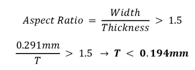
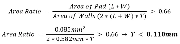
The calculation outlined in Figure 1 is critical for repeatable solderability. Aspect and area ratios should be kept to at least 1.5 and 0.66 respectively. This will ensure proper release of the solder paste release from the stencil without under pasting the part.
Example Calculation
Below is an example calculation of the stencil thickness using the recommended paste pattern from a PolyStrata RF launch:

Paste Type
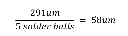
In addition to stencil thickness, the correct paste type should be used for good stencil release. IPC guidelines recommend the “five‑ball rule” — the solder paste ball size should allow for five solder balls to fit in the minimum aperture window.
| Type | Less than 0.5% larger than | 10% Max. between | 80% Min. between | 10% Max. less than |
|---|---|---|---|---|
| 1 | 160 | 150–160 | 75–150 | 75 |
| 2 | 80 | 75–80 | 45–75 | 45 |
| 3 | 60 | 45–60 | 25–45 | 25 |
| 4 | 50 | 38–50 | 20–38 | 20 |
| 5 | 40 | 25–40 | 15–25 | 15 |
| 6 | 25 | 15–25 | 5–15 | 5 |
| 7 | 15 | 11–15 | 2–11 | 2 |
Figure 3 – Solder Paste Size by Type (microns)
Using our example RF pin launch, the minimum aperture size is 0.291mm:
Reflow Profiles
PolyStrata SMT components are compatible with standard leaded and non‑leaded reflow profiles. The choice of reflow profile should be dictated by the recommended reflow from the solder paste vendor. An example generic profile provided by Kester for their leaded and lead‑free solder pastes is shown below:

Pick and Place
All PolyStrata SMT components are compatible with standard pick and place assembly processes. It’s recommended to follow these precautions for proper placement:
- Keep fiducial references close to the PolyStrata component. The accuracy of the pick and place head is affected by distance traversed from the fiducial reference. Placing a fiducial reference close to the component minimizes this error.
- Reduce head speed during placement. With high head speeds, parts can slide along the vacuum head due to abrupt changes in speed as the head starts and stops — creating a translation error between the pickup and place point on the PCB. Reducing head speed reduces these errors.
- Use copper alignment features instead of silkscreen. Solder mask and copper alignment are generally much more accurate than silkscreen, so it can be beneficial to use copper alignment features on the board for optical inspection:

Figure 5 — Copper Alignment PCB Feature - Use the proper pickup location and size for the component, as outlined in the interface control drawing:

Figure 6 — Vacuum Pickup Area
Footprint
Part footprints are available in DXF and native Altium Designer formats on request — reach out to your Nuvotronics representative to receive these files. Alternatively, a footprint can be made from the mechanical model of the PolyStrata part. Follow the layer expansion guidelines below when creating a footprint for PolyStrata components:

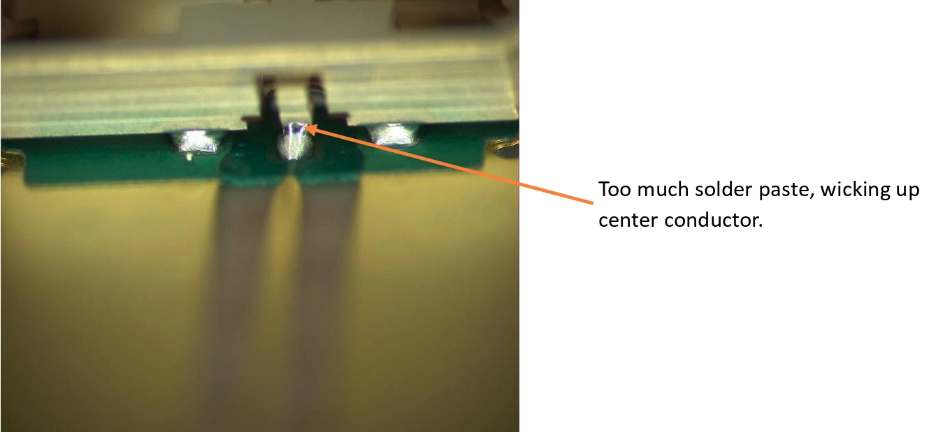
Examples
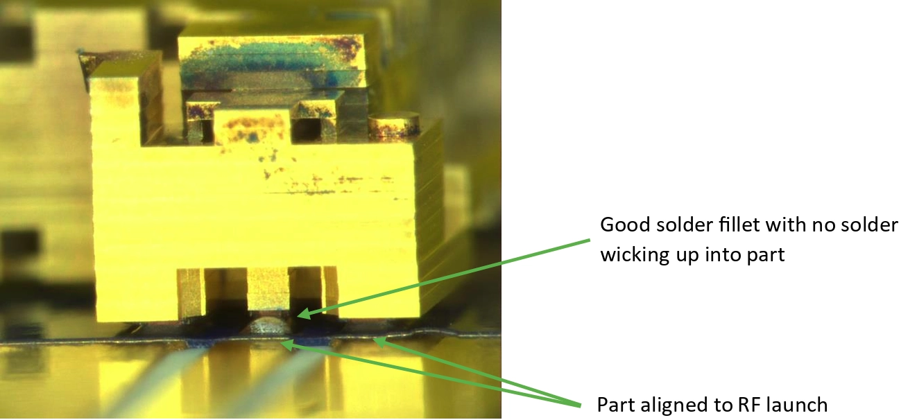
Figure 8 — Good Solder Example
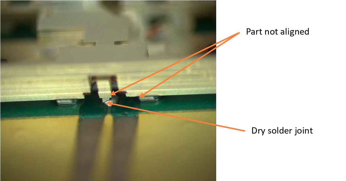
Figure 9 — Alignment Error